MYSHOP
최근 본 상품


| 상품명 | DRV8833 Dual Motor Driver Carrier |
|---|---|
| 판매가 | 20,364원 |
| 적립금 | 200원 (1%) |
| 상품코드 | P000EBWF |
| 수량 |   |
| 세액 | 2,036원 |
| 공급사 | Pololu |
| SNS 상품홍보 |
|---|

 |
(최소주문수량 1개 이상 / 최대주문수량 0개 이하)
사이즈 가이드 수량을 선택해주세요.
위 옵션선택 박스를 선택하시면 아래에 상품이 추가됩니다.
| 상품명 | 상품수 | 가격 |
|---|---|---|
| DRV8833 Dual Motor Driver Carrier |   |
( |
총 상품금액(수량) : 0 (0개)

|
||
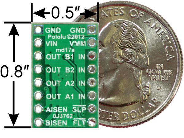 |
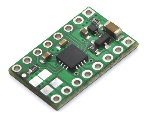
DRV8833 dual motor driver carrier, bottom view with dimensions. |
|---|
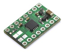
Texas Instruments’ DRV8833 is a dual H-bridge motor driver IC that can be used for bidirectional control of two brushed DC motors at 2.7 V to 10.8 V. It can supply up to about 1.2 A per channel continuously and can tolerate peak currents up to 2 A per channel for a few seconds, making it an ideal driver for small motors that run on relatively low voltages. Since this board is a carrier for the DRV8833, we recommend careful reading of the DRV8833 datasheet(1MB pdf). The board ships populated with SMD components, including the DRV8833, and adds a FET for reverse battery protection.
This board is very similar to our DRV8835 dual motor driver carrier in operating voltage range and continuous current rating, but the DRV8835 has a lower minimum operating voltage, offers an extra control interface mode, and is 0.1″ smaller in each dimension; we also carry a DRV8835 dual motor driver shield that is easy to use with an Arduino. The DRV8833 has a higher peak current rating (2 A per channel vs 1.5 A), optional built-in current-limiting, and no need for externally supplied logic voltage.
For a smaller, lower-cost, single-channel alternative to this driver, please consider our DRV8838 carrier, which offers a similar operating voltage range and current capabilities.
For higher-voltage alternatives to this driver, consider our A4990 and DRV8801 motor driver carriers.
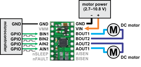 |
Minimal wiring diagram for connecting a microcontroller to a DRV8833 dual motor driver carrier. |
|---|
In a typical application, power connections are made on one side of the board and control connections are made on the other. The nSLEEP pin is pulled high on the board and can be left disconnected if you do not want to use the low-power sleep mode of the DRV8833. Each of the two motor channels has a pair of control inputs, xIN1 and xIN2, that set the state of the corresponding outputs, xOUT1 and xOUT2; pulse width modulated (PWM) signal can be applied to each of these inputs. The control inputs are pulled low internally, effectively disabling the motor driver outputs by default. See the truth tables in the DRV8833 datasheet for more information on how the inputs affect the driver outputs.
The nFAULT pin is an open-drain output that is driven low by the chip whenever an over-current, over-temperature-or under-voltage condition occurs. Otherwise, it remains in a floating state, so you will need to connect an external pull-up resistor (or use a microcontroller input with its built-in pull-up enabled) if you want to monitor fault conditions on the driver.
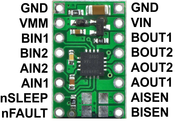 |
| PIN | Default State | Description |
|---|---|---|
| VIN | Reverse-protected 2.7 V to 10.8 V motor power supply connection. Operation with VIN below 5 V slightly reduces the maximum current output. | |
| VMM | This pin gives access to the motor power supply after the reverse-voltage protection MOSFET (see the board schematic below). It can be used to supply reverse-protected power to other components in the system. It is generally intended as an output, but it can also be used to supply board power. | |
| GND | Ground connection points for the motor power supply and control ground reference. The control source and the motor driver must share a common ground. | |
| AOUT1 | The motor A half-bridge 1 output. | |
| AOUT2 | The motor A half-bridge 2 output. | |
| BOUT1 | The motor B half-bridge 1 output. | |
| BOUT2 | The motor B half-bridge 2 output. | |
| AIN1 | LOW | A logic input control for motor channel A. PWM can be applied to this pin. |
| AIN2 | LOW | A logic input control for motor channel A. PWM can be applied to this pin. |
| BIN1 | LOW | A logic input control for motor channel B. PWM can be applied to this pin. |
| BIN2 | LOW | A logic input control for motor channel B. PWM can be applied to this pin. |
| nSLEEP | HIGH | Sleep input: when this pin is driven low, the chip enters a low-power sleep mode. (Labeled SLP on the board silkscreen.) |
| nFAULT | FLOAT | Fault output: driven low in the event of an over-current, over-temperature, or under-voltage condition; floating otherwise. (Labeled FLT on the board silkscreen.) |
| AISEN | Current sense pin for motor A. This pin is connected to ground and does not function by default, but current limiting can be enabled by making the modifications described below. | |
| BISEN | Current sense pin for motor B. This pin is connected to ground and does not function by default, but current limiting can be enabled by making the modifications described below. |
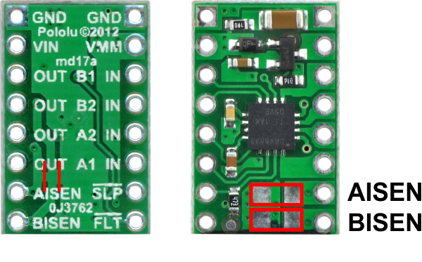
The DRV8833 can actively limit the current through the motors by using a fixed-frequency PWM current regulation (current chopping). By default, this carrier board connects the current sense pins to ground, disabling the current limiting feature. To enable current limiting, you can use a knife to cut the break points on the back of the board and then solder some appropriate current sense resistors to the unpopulated pads on the front, as indicated in the image below. The pads are sized for 1206 surface-mount resistors. Refer to the DRV8833 datasheet for information on how the resistor value determines the chopping current.
 |
The DRV8833 datasheet recommends a maximum continuous current of 1.5 A per motor channel. However, the chip by itself will overheat at lower currents. For example, in our tests at room temperature with no forced air flow, the chip was able to deliver 1.5 A per channel for about a minute before the chip’s thermal protection kicked in and disabled the motor outputs, while a continuous current of 1.2–1.3 A per channel was sustainable for many minutes without triggering a thermal shutdown. The actual current you can deliver will depend on how well you can keep the motor driver cool. The carrier’s printed circuit board is designed to draw heat out of the motor driver chip, but performance can be improved by adding a heat sink. Our tests were conducted at 100% duty cycle; PWMing the motor will introduce additional heating proportional to the frequency.
This product can get hot enough to burn you long before the chip overheats. Take care when handling this product and other components connected to it.
|
|
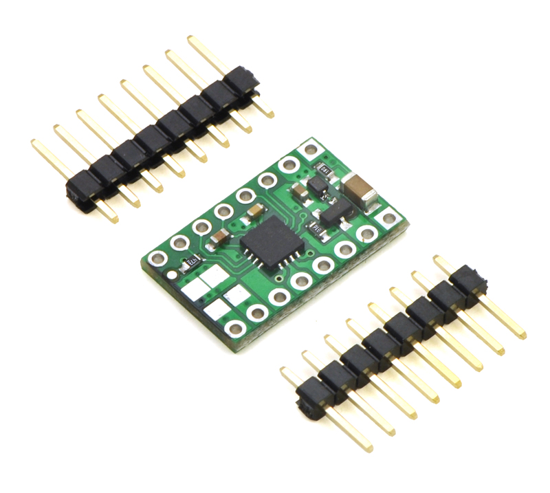
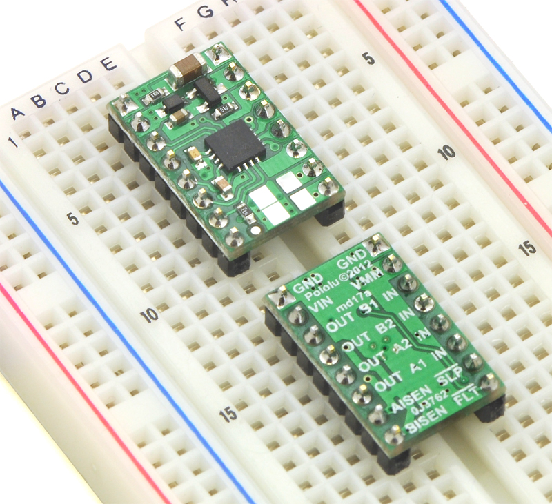
Two 1×8-pin breakaway 0.1″ male headers are included with the DRV8833 dual motor driver carrier, which can be soldered in to use the driver with perfboards, breadboards, or 0.1″ female connectors. (The headers might ship as a single 1×16 piece that can be broken in half.) The right picture above shows the two possible board orientations when used with these header pins (parts visible or silkscreen visible). You can also solder your motor leads and other connections directly to the board.
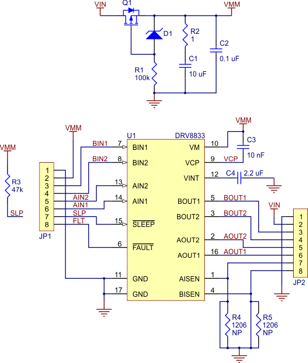 |
Schematic diagram of the DRV8833 dual motor driver carrier. |
|---|
* 세금계산서 발행방법은 게시판 공지사항 참조.
* 기술문의는 이메일(master@toolparts.co.kr)로 문의.
전자부품 특성상 제품에 이상이 있거나, 상품정보와 상이한 경우 외 에 단순 고객변심으로는
교환 반품이 불가능 합니다 구매전 이점 유의해 주세요!!!
고액결제의 경우 안전을 위해 카드사에서 확인전화를 드릴 수도 있습니다. 확인과정에서 도난 카드의 사용이나 타인 명의의 주문등 정상적인 주문이 아니라고 판단될 경우 임의로 주문을 보류 또는 취소할 수 있습니다.
무통장 입금은 상품 구매 대금은 PC뱅킹, 인터넷뱅킹, 텔레뱅킹 혹은 가까운 은행에서 직접 입금하시면 됩니다.
주문시 입력한 입금자명과 실제입금자의 성명이 반드시 일치하여야 하며, 7일 이내로 입금을 하셔야 하며 입금되지 않은 주문은 자동취소 됩니다.
교환 및 반품이 가능한 경우
- 상품을 공급 받으신 날로부터 7일이내 단, 가전제품의
경우 포장을 개봉하였거나 포장이 훼손되어 상품가치가 상실된 경우에는 교환/반품이 불가능합니다.
- 공급받으신 상품 및 용역의 내용이 표시.광고 내용과
다르거나 다르게 이행된 경우에는 공급받은 날로부터 3월이내, 그사실을 알게 된 날로부터 30일이내
교환 및 반품이 불가능한 경우
- 고객님의 책임 있는 사유로 상품등이 멸실 또는 훼손된 경우. 단, 상품의 내용을 확인하기 위하여
포장 등을 훼손한 경우는 제외
- 포장을 개봉하였거나 포장이 훼손되어 상품가치가 상실된 경우
(예 : 가전제품, 식품, 음반 등, 단 액정화면이 부착된 노트북, LCD모니터, 디지털 카메라 등의 불량화소에
따른 반품/교환은 제조사 기준에 따릅니다.)
- 고객님의 사용 또는 일부 소비에 의하여 상품의 가치가 현저히 감소한 경우 단, 화장품등의 경우 시용제품을
제공한 경우에 한 합니다.
- 시간의 경과에 의하여 재판매가 곤란할 정도로 상품등의 가치가 현저히 감소한 경우
- 복제가 가능한 상품등의 포장을 훼손한 경우
(자세한 내용은 고객만족센터 1:1 E-MAIL상담을 이용해 주시기 바랍니다.)
※ 고객님의 마음이 바뀌어 교환, 반품을 하실 경우 상품반송 비용은 고객님께서 부담하셔야 합니다.
(색상 교환, 사이즈 교환 등 포함)
상품의 사용후기를 적어주세요.
게시물이 없습니다


상품에 대해 궁금한 점을 해결해 드립니다.
게시물이 없습니다